Cpr
E 282x Laboratory
Lab 3a
Hardware I/O
The objective of this lab is to develop an understanding of how the PowerBox microcontroller handles input and output (I/O). You will program the PowerBox to take a 3-bit digital input and output a sum and carry to the dual 7-segment display. You will also represent the 3-bit input on a led bargraph. To accomplish this you will modify your adder program from lab 2 and program the microcontroller to handle this I/O.
Reference Files for Lab
I/O on the PowerBox
First you will need to learn a little about I/O on the PowerBox. Carefully read the following section. There is a lot of good information and some of it you may be unfamiliar with. If you don’t understand something please bring it to your TA’s attention.
You have seen a fairly limited view of the Power PC board and how it interacts with the real world. In this section, you will learn a few more details about the PowerBox digital I/O components. To begin, here is some helpful terminology:
- Bus - A collection of wires sharing a common purpose
- Latch - A flip-flop used to keep data, stores data on a signal and holds the data until the next signal is received
- Buffer – Stores and transfers data, typically having outputs in three possible states (low, high, or high impedance (open circuit))
In order to read/write data to the outside world, the PowerPC processor sends signals on a collection of wires known as a bus. The three main bus types for any computer system are:
- Address - Who is the processor talking to (RAM, ROM, hard disk, temperature sensor, etc.)?
- Data - What is being said (110.6 degrees, 0xFA, "Hello")?
- Control - Who is doing the talking (device, processor)?
Now, the PowerPC processor is not set up by default to interact with the real world. Thus, we need some components to help the processor interface with the real world. This introduction is primarily concerned with the digital input and output components of the PowerBox.
Memory-Mapped I/O
The PowerBox uses what is known as memory-mapped I/O. Essentially,
memory-mapped I/O can be summarized as simply putting all devices and memory
out in a large memory space. Thus, when you are using pointers to read
and write to memory locations, you may be using different devices. For
instance, memory address 0x2000 may point to a serial port, whereas 0x3000 may
be in a block of
- 0x20000000 - RAM - 16 MB of memory
- 0x40000000 - Digital Input/Output
You will be writing the code for accessing the digital input/output. You will use constants defined in the file defines.h, shown partially below.
//
Defines.h : Definition file for PowerBox
/////////////////////////////////////////////////////////////////////////
//
Overall memory addresses for external I/O board
// 32 bit pointer
//
#define ADDRESS_START_EXT_RAM 0x20000000
#define ADDRESS_START_EXT_IO 0x40000000
/////////////////////////////////////////////////////////////////////////
// I/O
ports
//
// All I/O ports are 8 bit ports
//
#define
IO_DIGITAL_INPUT_1 0x40000003
#define
IO_DIGITAL_INPUT_2 0x40000007
#define
IO_DIGITAL_INPUT_DIP_1 0x4000000B
#define
IO_DIGITAL_INPUT_DIP_2 0x4000000F
#define
IO_DIGITAL_INPUT_KEYPAD 0x40000013
#define
IO_DIGITAL_OUTPUT_LED1 0x40000023
#define
IO_DIGITAL_OUTPUT_LED2 0x40000027
#define
IO_DIGITAL_OUTPUT_1 0x4000002B
#define
IO_DIGITAL_OUTPUT_2 0x4000002F
#define
IO_DIGITAL_OUTPUT_7SEG 0x40000033
#endif
Digital Input
To read information in from the external I/O board, the PowerPC processor does a read to a memory address in the 0x40000000 memory address space. The circuitry for the digital input circuit looks something like the following:

The outside world digital source may come into the PowerBox via either the DIP switch or the Digital Input channels as digital signals. The data itself is transmitted to the CPU via the data bus. However, the CPU uses the data bus for more than just reading digital input. Thus, a buffer chip is required that places information on the data bus only when it is requested by the CPU. When the CPU wishes to read information from one of the digital inputs, it signals the buffer chip to allow it to change the data bus. The chip changes the data bus and the CPU reads the data bus to get the value of the digital input.
The buffer chip serves a second purpose as well. On the data bus, there are several devices waiting to read/write to the bus. On the PowerBox, there are 10 different input/output ports. However, what happens if each of the devices tries to talk at once. Suppose one device drives a data pin with +5V and another device assigns it 0 V. Who wins? In this case, nobody. The system ends up having nonsense most of the time and does not work.
The solution is to place the outputs of devices that are NOT talking on the bus into a high impedance state (i.e., looks just like an open circuit). Such a device is effectively disconnected from the bus. By doing so, all of the devices can share the bus and take turns using it as specified by the CPU.
Digital Output
The digital output case is fairly similar with a small twist. Instead of waiting to change the data bus, the output circuits receive their values from the data bus. Since the data bus is used for many different purposes, will the data bus contain the desired output value? The answer is no. Therefore, we need to include a latch in the circuit as pictured below:

A latch is essentially a flip-flop (or set of flip-flops). Most latches come in 4- or 8-bit blocks. The latch is used to store the value and keep writing out the same value until the CPU changes it. Think about the LED bargraph and the 7-segment displays. Although the program is updating the output once a second, the latch is what keeps the same value being displayed when the CPU is doing other things.
DIP Switch Input
The DIP switches on the PowerBox are connected in the following manner:

The resistors in the circuit are known as pull-down resistors. With the pull-down resistors, each switch value is forced to be either a +5V or a 0V due to the voltage drop across the resistor.
When the DIP switch is open, there is not a connection. There is no connection to +5 V and the line stays at ground (Logic 0). When the DIP switch is closed, current flows from Vcc (+5 V) to ground and the line rises to +5 V. Notice the connection to ground is key to forcing the line to appropriate values. The pull-down resistor prevents a direct connection from Vcc (+5 V) to ground.
LED Output
In order to power LEDs, there are two choices, acting as a source for the current or acting as a sink for the current. However, if you look at TTL logic sheets (see TI's website), you will notice that ratings are given for both current sourcing as well as current sinking. Typically, the chip is able to sink significantly more current than it is able to source. One must take special care when designing a circuit not to violate the maximum current constraints of the chip, otherwise you will burn out the chip.
In a current sink setup, the TTL chip varies between +5 V or 0 V. The LED receives +5 V. The TTL chip varies its output between +5 V and 0 V to either turn off or light the LED.
When the TTL chip outputs a +5 V, the voltage difference between the +5 V (Vcc) and the TTL chip is 0 (5 V - 5 V = 0). Hence, no current flows and the LED does not light.
If the TTL chip outputs 0 V, the voltage difference becomes 5 V (5 V - 0 V = 5 V). Hence, current flows and the LED lights correctly.

For the above scenario, notice that a resistor is included in the diagram as well. The resistor is known as a current-limiting resistor and is critical to the correct operation of the circuit. Without it, current would flow directly from +5 V into the TTL chip at a level far beyond what the chip can handle. Think of it this way, if you connect Vcc and ground (don't do it), what happens? Bad things of course, you have a short circuit. By placing a current-limiting resistor between Vcc and ground, the current is limited to an appropriate level. Remember, I (Current) = V (Voltage) / R (Resistance). How much current flows if you use a 270 Ohm resistor?
7-Segment Output
The 7-segment display operates in a similar fashion to the LED bargraph. However, the 7-segment display circuit uses a 7-segment decoder to translate from a 4-bit binary value (0000 to 1111) to a 7-segment representation of the respective hex digit (0 to F). The decoder takes 4 inputs and maps them onto 7 outputs (pins a-g). For the PowerBox, the 7-segment display includes a built-in resistor.

Be ready to discuss the digital input/output ports with your TA as you proceed to use them in the rest of the lab.
Create a new CodeWarrior project
In CodeWarrior click on File à New… Then select “CprE 282x – PowerPC 555 Stationery”. For the ‘Project Name:’ type “lab3a”. For the ‘Location’ click on the ‘Set…’ button and go to your Labs folder where you saved labw01b. Type “lab3a” as the ‘File Name:’ and click on ‘Save’. CodeWarrior will create a labw02b folder for your project. Now click ‘OK’ in the ‘New’ window. A prompt asks you to select project stationery. Select ‘C code’ and click ‘OK’. You have now created a new project for labw02b.
Now you are ready to
code…
In the ‘lab3a.mcp’ window expand ‘C Source Files’. Double-click main.c to open it.
To begin you will need to include the ‘defines.h’ header file you read about under Memory Mapped I/O. The actual header file has already been added to Misc. Source files for you, but it still needs to be included in your main.c program. Just add one more include statement:
#include "defines.h"
Next you will need to access the different I/O devices on the PowerBox. Because the I/O is “memory mapped”, simply reading the value at memory location 0x4000000B will give you the value of DipSwitch1. Rather than memorizing which address goes with which device the ‘defines.h’ file defined these addresses for you, (e.g. IO_DIGITAL_INPUT_DIP_1 is defined as address 0x4000000B). Now we can setup our own pointers to access these defined locations. To do this add the following lines right after your include statements.
char * pDIPSwitch1 = (char *)
IO_DIGITAL_INPUT_DIP_1;
char * pLEDBargraph2 = (char *)
IO_DIGITAL_OUTPUT_LED2;
char * pLEDBargraph1 = (char *)
IO_DIGITAL_OUTPUT_LED1;
char * p7SEG = (char *)
IO_DIGITAL_OUTPUT_7SEG;
Now, to get the input from, say dipswitch1 for example, we
would read the memory location pointed to by pDIPSwitch1. For
example:
char dip1value = *pDIPSwitch1;
The value stored in memory, and thus the value written to dip1value is an 8 bit “character” data type or ‘char’ in c. Each bit in the character represents one of the dipswitches. For example if the dipswitch 1 is set to:
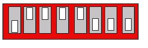
The value stored in memory at address 0x4000000B is b01111000, or 0x78 in hexadecimal.
NOTE: When you flip the dipswitches, only the value stored in memory changes. You will have read the pointer again to update the value in your program.
It is good practice to give your outputs a starting state, or initial value. The 2 bargraphs, and the 7-segment display should be turned off. Add the following in main:
//Initialize the LED Bargraphs and
the 7-segment display.
*pLEDBargraph1 = 0xFF; //Turn
off all LEDs on bargraph
*pLEDBargraph2 = 0xFF; //Turn
off all LEDs on bargraph
*p7SEG = 0x00; //Turn
off the 7-segment display
Why are we writing 2 different values to these devices if we want them all to do the same thing?
Now you will need to an infinite loop so that the microcontroller is continuously scanning the inputs and producing output.
while(1)
{
//Your
adder program here.
}
If you did not have such a loop what would happen?
Finally you are ready to enter the nested conditional version of your adder program from lab 2. You will need to read DipSwitch1 and assign the proper carry and sum values. These should be output to the dual 7-segment display. The left digit will represent the carry value, and the right digit will represent the sum value (display a ‘1’ or a ‘0’ for each case). Also, LED Bargraph1 should show the value entered on DipSwitch1. Hint: still try to use x, y, and z variables in your program.
Compiling and running
the program…
To compile your program and check for errors select Project à
Make. Then select Project à
Enable Debugger (you will only need to do this once). Then select Project à
Debug. The ‘PowerPC.elf’ window pops
up and the program is downloaded to the microcontroller. To run it select Project à
Run. To stop it at any time select Debug à
Kill.
If you are having trouble with your program there is a wonderful feature for the PowerBox and CodeWarrior…the Debugger. It allows you to step through your code and execute line by line. You must be running in “debugging” mode, which up to this point that is exactly what you’ve been doing. That is why you were instructed to enable the debugger. To step through your code select Project à Debug. Once the ‘PowerPC.elf’ window is ready select Debug à Step Over or (F10). Now try this on your program and observe the top two portions of the ‘PowerPC.elf’ window and the output devices on the PowerBox.
You’re done! Turn in your Lab Evaluation Form to your TA.