CPR E 281x/282x - Lab 4b
2’s
Compliment Addition with a Ripple-Carry Adder
&
Introduction
to Verilog in Quartus II
1. Objectives
In the previous lab you
learned how to design digital circuits by drawing schematics in the graphic
editor. In this lab you will design two
circuits and for each circuit you will use the graphic editor to create the
circuit. Then you will duplicate that
circuit using Verilog. You will first
design a 1-bit full adder. Then you will
use 8 full adders to make an 8-bit ripple-carry adder for 2’s complement
addition.
1.1 Reference Files for Lab
2. Prelab
Before you come to lab it will be useful to become familiar with a full
adder, 2’s complement, a ripple-carry adder, and Verilog. All of which is covered in chapter 5 of your
text “Fundamentals of Digital Logic with
Verilog Design” by Brown and Vranesic.
Specific sections of the text that are related to each circuit will be
listed at the beginning of each section of the lab.
3. Setup
As you did in previous labs, make sure you create the
folder in your home directory U:\CPRE281\Lab04b,
and then four sub-folders \adder_1bit,
\adder_1bit_gates, \adder_8bit, and
\adder_8bit_gates. It is important
that you use these folder names.
4. Full adder in schematics
Refer to the
textbook from step 2: Section 5.2.
Begin by starting up Quartus II.
Create a new project in the U:\CPRE281\Lab04b\adder_1bit_gates
folder. Create a new .bdf file named adder_1bit_gates.bdf, and
add it to the project. Now you are ready
to draw your schematic of a 1bit full adder.
Refer to Figure
5.4 (page 237) in the text.
Name the inputs ina,
inb, and cin. Name the outputs sum and cout. Use the waveform editor to view the input and
output. Verify that your adder is
working as expected, and then show the TA your results.
Next you need to turn your
1bit adder into a part, or symbol, that you can use to build an 8bit
adder. In order to make a symbol, click
on File à Create/Update àCreate Symbol Files for Current File. A box should
appear informing you that a symbol was created for this part, ‘adder_1bit_gates.bsf’.
5. Full adder in Verilog
Refer to the
textbook from step 2: Section 5.5.2.
Begin by creating a new project in the U:\CPRE281\Lab04b\adder_1bit
folder. Create a new Verilog HDL file. Next you need to save this file. Select File à Save As… and
the ‘File Name’ should be “adder_1bit.v” and save this file in the ‘adder_1bit’
folder, click OK. Next select the adder_1bit in the project
navigator window, right click, and select Set as Top-Level Entity. Now you are ready to create a 1bit full adder
module in Verilog. Refer to Figures 5.23, 5.24,
5.25, and 5.26
(pages 265, 266) in the text.
There are two different ways to write this code. One is to use gate level primitives and the
other is to use functional expressions.
Choose either way for your design.
Name the inputs ina,
inb, and cin. Name the outputs sum and cout. When you are finished writing code, the steps
for saving, compiling, and simulating are the same as they were for a schematic
design. Use the waveform editor to view
the input and output. Open up the ‘adder_1bit_gates.vwf’
file from step 4 and compare the outputs to make sure they are the same. Show the TA your results.
6. Ripple-carry adder in schematics
Refer to the
textbook: Sections
5.2.2, 5.3, 5.3.1(2’s
Comp.),
5.3.2(2’s Comp. Addition), and 5.3.5 (starting
on page 239).
Create a new project in the U:\CPRE281\Lab04b\adder_8bit_gates
folder. Create a new .bdf file named adder_8bit_gates.bdf, and
add it to the project. Now you are ready
to draw your schematic of an 8bit ripple-carry adder.
In order to use the adder_1bit symbol you created previously you will
need to copy the ‘adder_1bit_gates.bsf’,
and ‘adder_1bit_gates.bdf’
files from the ‘adder_1bit_gates’
folder to the ‘adder_8bit_gates’
folder. To use the symbol go to Enter Symbol…, in
name field, clock …and
browse to ‘~\lab04b\adder_8bit_gates’,
and select the ‘adder_1bit_gates.bsf’
symbol.
Creating 17 different input pins and wiring each one individually can
be very time consuming and will make your schematic hard to read. Think of how many pins you would need for
adding two 32bit numbers. A more
efficient way to wire them is to group the common inputs, or outputs, together
into buses. Then you only need to run
one bus wire and take individual pins off of it wherever they are needed. This also means for this project you only
need 3 input pins: 2 for bus inputs and 1 pin for cin.
To create the bus wires, we will name the inputs A[7..0], B[7..0]. If you draw a wire from the end of the input
you should notice that it is thicker than a normal wire to indicate it is a
bus. Now you need to connect each
individual 1-bit adder instance to the buses for A and B. Each connection needs to be named so that
Quartus knows which wire in the bus is connected to that 1-bit adder. To do this, click on the wire connecting the
bus, and while it is highlighted type the name of the wire. For the A input
bus, the names will range from A[0] to A[7].
An example of the first 1-bit adder is shown below:
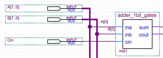
NOTE: The
name A[0] may appear anywhere along the wire, depending on where you clicked to
select the wire. As long as clicking on
the wire highlights both the wire and the name, you should be set.
From the picture you will
notice that a third input, Cin is
necessary.
Combine the sum outputs of the 8 1-bit adders into a bus by creating an
output sum[7..0],
then connecting the individual outputs to the bus as above. You will need two additional output pins, cout and oflow,
used to indicate carry out and overflow respectively. Refer to section 5.3.5 on
how to detect an arithmetic overflow when performing addition.
Use the waveform editor to view the input and output. When adding the nodes to the waveform, select
A, B, and sum, and
not the individual wire A[0], A[1], …, B[0], sum[0], etc. This will keep the wires grouped into buses
inside the waveform. You may still view
the individual wire components by clicking on the + sign next to the bus name,
and in addition, with the bus wire grouped in this manner, you may assign the
entire bus a value. E.g. you can assign
the input A the value 57, but if not grouped, you would have to assign A[5],
A[4], A[3], and A[0] the value 1, and the rest 0 to achieve a value of 57 for
the bus.
Assign the inputs values that will assert both the cout and oflow
outputs. Show the TA your results.
7. Ripple-carry adder in Verilog
Refer to the
textbook: Section
5.5.3 (page 268).
Once again, begin by creating a new project in the U:\CPRE281\Lab04b\adder_8bit
folder. Create a new Verilog HDL file. Next you need to save this file. Select File à Save As… and
the ‘File Name’ should be “adder_8bit.v” and save this file in the ‘adder_8bit’
folder, click OK. Next select the file adder_8bit in the
project navigator window, right click, and select Set as Top-Level Entity. Now you are ready to create an 8bit
ripple-carry adder module in Verilog.
For this module, duplicate the schematic you created in the last
step. You will use 8 instances of the
adder_1bit module you created in step 5.
The instances will need to be connected to each other. Refer to Section 5.5.3 and Figure 5.28 in
the text for an example of how to create 4 instances of a 1-bit adder and
connect them together. In general the
format for declaring an instance (or part) in Verilog is:
Module_name Instance_name (inputs and outputs)
In this case, the Module_name is adder_1bit. You may choose Instance_name however you like, but it must be unique for every
instance. Finally the inputs and outputs
will be connected in the same order as they are declared in the Module_name.v file.