CPR E 281x/282x - Lab 6a
Decoders
in schematics and Verilog
1. Objectives
In this lab you will design
a 2 to 4, and a 4 to16 decoder. Both
circuits will be designed in Verilog.
Then you will construct a BCD to 7-segment decoder, and use it in a circuit.
1.1
Reference Files for Lab
2. Prelab
Before you come to lab it
will be useful to become familiar with decoders. You will find information on decoders in
section 6.2 of your text: “Fundamentals
of Digital Logic with Verilog Design” by Brown and Vranesic.
3. Setup
As you
did in previous labs, make sure you create the folder in your home directory U:\CPRE281\Lab6a, and then three
sub-folders ~\dec_2to4, ~\dec_4to16, and ~\bcd_7seg_dec. It is
important that you use these folder names.
Each module needs to be in its own folder. Then download the ‘addition_calc.zip’ file to your ~\Lab6a folder and extract it.
4. Decoder design in schematics
Look at each of the three following decoder
designs. Fill out the corresponding
tables on the answer sheet. For the 4 to
16 decoder write down which output is selected.

1 to 2 decoder
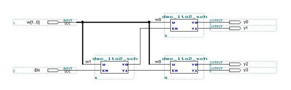
2 to 4 decoder

4 to 16 decoder
5. Designing decoders in Verilog
Begin with a 2 to 4 decoder
using case statements. Then build a 4 to 16 decoder,
(hierarchical). You will find helpful
information in section 6.6 of the text.
You will need to provide the waveform results for the 4 to 16
decoder. The grid size can be adjusted
so that you can fit more input values in the window (Edit à Grid Size…). Be selective when adding nodes to the
waveform editor. Show the TA both
modules and the waveform results for the 4 to 16. Once your 4 to 16 is correct, create a symbol
for it.
6. Design a BCD to 7-segment decoder
in Schematics
Use a 4 to 16 decoder
and OR gates to create a BCD to 7-segment decoder. You will find information on them, as well as
a truth table, in section 6.4 of the text (pp. 318-319). You will need a lot of space to draw this
schematic. Keep your wiring neat and
organized. The TA will explain the
operation of the 7-segment display and how to read the truth table. Show the TA the design and waveform results
for the BCD to 7-segment decoder. Once
your BCD to 7-segment decoder is correct, create a symbol for it.
7. Use the BCD to 7-segment decoder
in a circuit
To better demonstrate
the output of your BCD to 7-segment decoder you will use it in a simple adder
circuit so you can view it in hardware.
A skeleton schematic has been provided for you (addition_calc.qpf). You will need to add your BCD to 7-segment
decoder, and one 4-bit adder.
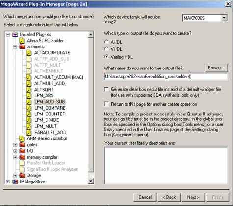
To create the 4-bit
adder select ‘Edit à Insert Symbol’ and
click MegaWizard Plug-In Manager…. Then select ‘Create a new custom megafunction
variation’. In the next window choose ‘LPM_ADD_SUB’, ‘VerilogHDL’, and give the file path and name “~\lab6a\addition_calc\adder4” as shown below.
In the next window
make the input 4 bits wide, and
select addition only. In the next window select No.
In the next window there will be no carry. In the next window select No.
In the final window click ‘Finish’. Now you can enter the adder4 symbol into the
schematic.
Complete the circuit
and compile the design. The Pin assignments
have already been done for you, however you will need make sure that the board
is wired correctly so that you are using the dipswitches for inputs inA and inB.
Refer to Lab 2a as necessary. Program the board with your design and verify
that it is functioning correctly. Show
the TA your adder and tell your TA why the hardware does not display 8+2=A.