
Figure 1 : EPM7128SLC84-7 Device Prototyping Header Pin Assignment
Computer Engineering 210 is an introductory class to the world of digital design. The laboratory exercises are intended to reinforce your understanding of classroom material with the use of computer as an experimental environment. The computer-aided-design tool we will be using this semester is MAX+PLUS II version 9.21 by ALTERA Corporation. The lab materials used are modified or partially reedited for use with MAX+PLUS II based on original work by Dr. Charles Wright.
We will be using an Altera MAX FPGA device, EPM7128SLC84-7, for our exercises. The next section describes the pin layout for MAX+PLUS II Prototyping Headers. The following section is the pin assignments for the MAX_DIGIT display, which are pre-wired to the prototyping headers. These information will be needed when a design is to be downloaded and tested using the Altera University Program (UP1) Education Board. The remaining of the manual are the lab sessions that are to be completed by the students.
The laboratory sessions will officially starts on the second week of
the semester in room 1318 Coover Hall.
EPM7128S Prototyping Headers Pin Assignments
The EPM7128S device is located in
an 84-pin plastic J-lead chip carrier (PLCC) package. There are a total
of 21 pins on each side of this 84-pin PLCC package, which are connected
to one of the 22-pin, dual-row 0.1-inch female headers. Since there are
only 21 pins on each side of the device, there is an unassigned pin on
each side of the connector. The pin numbers for the EPM7128S device are
shown as follows :
Figure 1 : EPM7128SLC84-7 Device Prototyping Header Pin Assignment
|
|
Unconnected pins ( unavailable for use ) |
| Reserved pins ( not modifiable ) | |
| JTAG signal pins ( unavailable for use ) | |
| Unassigned pins |
MAX_DIGIT Displays Pin Assignments
The dual-digit
seven-segment display is pre-wired directly to some of the I/O pins of
EPM7128S device. The LED segments of the display are all active LOW, illuminating
when driven by a logic 0. The segments of the display are named a, b, c,
d, e, f, and g, as shown in the diagram below. The pin assignments are
also given in the table below.
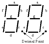
Figure 2 : MAX_DIGIT Display Segment Locations
| MAX_DIGIT Segment I/O Connections | ||
|
|
|
|
|
|
|
|
|
|
|
|
|
|
|
|
|
|
|
|
|
|
|
|
|
|
|
|
|
|
|
|
|
|
|
|
Table 1 : Pin Assignment
for MAX_DIGIT Display Segments
Authored by Jim Eng NG (©1999) for use with ALTERA
MAX+PLUS II Software and ALTERA UP1 Education Board