Lab
7
CprE
305
1.
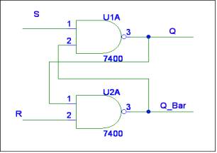
An
SR Latch is shown below. When S (set)
and R (reset) are both logical 1, the values on Q and Q_bar remain the same as
they were previously. When S goes to
logical 0, Q is set to 1 and Q_bar is the complement. S can then go back to logical 1, and the value at Q remains as
logical 1. Write the Verilog code for
the SR latch, SRlatch (S,R,Q,Qbar), using the same labels as the figure.
2.
An
SR latch can be used to store a value of a logical variable. For this purpose,
it is more useful if a clock (control) signal can be used to trigger a change
of state in Q and Q_bar based on the value of input variable. We also want to specify the value. A clocked
latch is used for this purpose. In a clocked latch, the outputs can change only
when the inputs change AND the clock is asserted (a logic 1 or logic 0,
depending on type of logic used). In the figure below, we show a clocked latch.
In this figure when clock signal is at logic 1, S and R input are asserted a
set of values depending on the value of D input. When clock signal is logic 0,
both S and R are at logic 1, keeping the old value of Q as it is. Write the
Verilog code for the D-latch, Dlatch(D, C, Q, Qbar), shown below.
3.
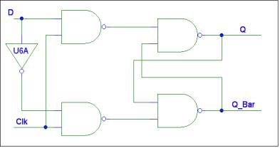
In
contrast to a latch, the output of a flip-flop only changes on a clock edge. The clock edge which affects can
be selected to be rising edge (clock signal going from 0 to 1) or fallong edge,
closck signal going from 1 to 0). This is realized using the circuit shown
below. Create the Verilog code for the rising-edge D-flip-flop, Dflipflop(D,
C, Q, Qbar), shown below by instantiating two D_latches and associated
circuitry. Notice that the circuit will be a falling-edge D-flip-flop if gate
U1A is removed.

4.
Write
the Verilog code for a 4-bit register, Reg4bit(D, C, Q), where D
and Q are 4-bit wide signals . A D flip-flop designed above can store 1
bit value. Your 4-bit register should
have a 4-bit input ([3:0] D), 1 clock input, C, and 4 outputs ([3:0] Q).
5.
A
register file is a key part of a microprocessor. It consists of a set of registers, each of which can be read from
or written to. For now, we will design
a register file, registerfile (datain, dataout1, dataout2, addra, addrb,
addrc, write, clock), that is capable of two simultaneous register
reads. Use Verilog to design a register
file with 4 registers, each of which is 4 bits wide. The 4 4-bit wide outputs from 4 registers will be connected to
two separate 4-to-1 multiplexors to produce two read outputs, dataout1
and dataout2, The two 2-bit wide control inputs to the two multiplexors,
addra and addrb, designate the two registers that will be
read. One 2-bit wide input, addrc,
decides which one of the four register will be written into if a control input,
write, is at logic 1 and rising edge of clock signal arrives. The
data to be written is provided by 4-bit input, datain. The TA will give
you sample inputs to be read from the registers.